
Micro Fabrication Facility Equipment

Wafer Cleaning & Wet Etching

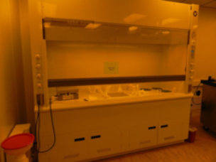
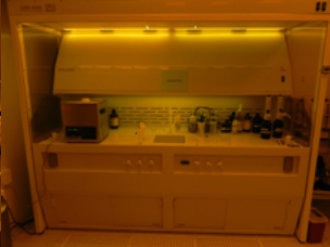
3 wet hoods from Salare Systems in NC for solvent, acid & base etching and wafer cleaning

  • Typical processes

    • NMP resist strip
    • RCA I & II cleaning
    • Piranha resist strip (NanoStrip 2X also available)
    • Chrome etch (CR-7)
    • Tungsten etch
    • Gold etch (GE 8148)
    • Platinum etch (Aqua Regia)
    • Nickel etch (HNO3 + Perfluoroalkyl Sulfonate)
  • acid-bench
    Acid Bench


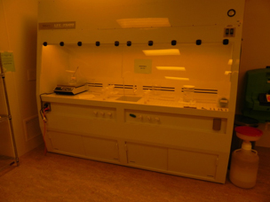
Additional Wet hoods

  • Sulfuric acid, Hydrogen Peroxide (Piranha Strip)
  • Hydrochloric Acid & Hydrogen Peroxide (RCA II cleaning)
  • Ammonium Hydroxide  &  Hydrogen Peroxide (RCA I  cleaning)
  • NMP, Acetone & Methanol (Solvents)
  • base-cleaning-bench
    Base Cleaning Bench
  • solvent-beach
    Solvent Bench

Resist Coating & Developing

  • Semi-automated resist coater with integrated hot plate
  • 100mm tooling
  • resist-caoter
    Resist Coater
  • developer-tool
    Developer Tool

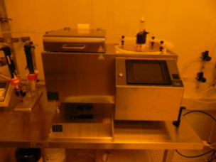
Brewer Sciences Photo Resist Developer Tool

  • Semi-automated wafer spin developer with integrated hot plate
  • 100mm tooling

UV Exposure

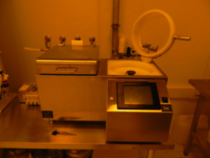
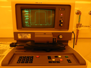
Nuetronix/Quintel 1X Contact/Proximity Printer

  • Model Q-7000-IR

    • 365nm exposure wavelength
    • Currently configured for 100mm wafers
    • Mask tooling for 4, 5 and 7”masks
    • Tooling available for 150mm wafers
    • IR back to front alignment capable
  • neutronix-quintel
    Neutronix-Quintel 1X Aligner
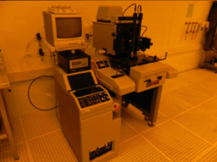
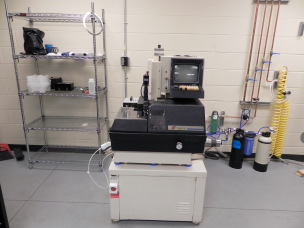
  • GCA 5:1 Reduction i-line optical stepper

    • 0.45na
    • 365nm exposure wavelength
    • Critical dimension (resolution) 0.5um
    • Overlay 150nm XBar + 3 sigma
    • Currently configured for 100mm dia. wafers, can expose up to 200mm wafers 0.25mm to 1.0mm thick
    • Customized Tooling for exposing 5” X 5” X  0.150” photomasks
    • Utilizes 5” X  5” reticles
    • Processing of piece/parts is possible with custom tooling
  • optical-stepper
    Reduction I-Line Optical Stepper

Plasma Etch

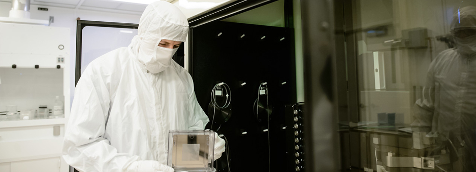
  • PlasmaTherm Versaline ICP

    • Fluorine gases for SiO2 and Si & Ge etching as well as other semiconductor materials
    • Configured for 100mm wafers up to 1mm thick
    • RIE and or ICP modes
    • Primarily used to dry etch SiO2 & Si films and bulk material
  • plasma-therm
    Plasma-Therm ICP
  • Oxford Instruments Plasmalab 100 ICP

    • Utilizes CL2 & BCL3 etch chemistry for metal or dielectric etching
    • Configured for 100mm wafers up to 1mm thick
    • Tool can etch up to 10mm thick wafers with optional tooling
    • RIE and or ICP modes
    • Currently used to dry etch Sapphire & Chromium 
  • oxford-plasmalab
    Oxford Plasmalab ICP

Dielectric Conformal Deposition

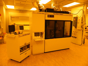
Atomic Layer Deposition (ALD)

  • Oxford Instruments OPAL ALD tool utilizing the following pre-cursors:

    • Diethyl zinc
    • Tetrakis(ethylmethylamino) hafnium (IV)
    • Titanium(IV) isopropoxide
    • Trimethylaluminum
  • oxford-ald
    Oxford ALD

Metal & Dielectric Deposition

Electron Beam Deposition

  • CCS CA-40 e-beam evaporator configured for 100mm wafers
  • Metals

    • Gold
    • Platinum
    • Nickel
    • Titanium
    • Chromium
    • Germanium
    • Palladium
    • Tantalum
    • Iron
  • Dielectrics

    • Tantalum Penta Oxide
    • Silicon Dioxide
    • Aluminum Dioxide
    • Silicon Monoxide
    • Titanium Dioxide
    • Hafnium Oxide
  • evaporator
    CCS-CA-40 Evaporator

Metrology

  • nikon-scope
    Nikon Scope
  • alpha-step
    Alpha Step
  • hitachi
    Hitachi SEM
  • film-thickness-tool
    Filmetrics F20 UV Optical Film Thickness Measurement System

Wafer Dicing

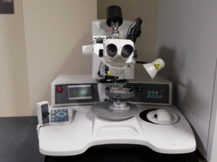
  • K&S Wafer Dicing Saw

    • Model 780
    • 200mm capable
    • Cuts silicon, sapphire & optical glasses
  • dicing-saw
    K&S Dicing Saw

Wire Bonding

  • K&S Wire Bonder

    • Model 4525AD
    • Gold wire 0.18um to 76um
    • Man & Auto
    • 152mm X 152mm area
  • wire-bonder
    K&S Wire Bonder

Custom Tooling

Custom tooling fees are charged on a tool by tool basis depending on the complexity of design and material needed.