Sputter Coaters
Two sputter coaters available for non-conductive or beam sensitive samples. Most of our SEMs allow for Variable Pressure imaging and can use low accelerating voltages, but in some cases higher quality or higher resolution imaging requires a thin coating (~1-10 nm).
- Reduced beam damage for sensitive specimen
- Increased conduction reduces sample charging
- Minimizes thermal damage from e- beam
- Improved edge resolution by reducing beam penetration
- All coatings have a higher electron yield and will increase signal to noise during imaging.
- Coating with lower atomic numbers is best for BSE imaging while higher atomic numbers is better for SE imaging
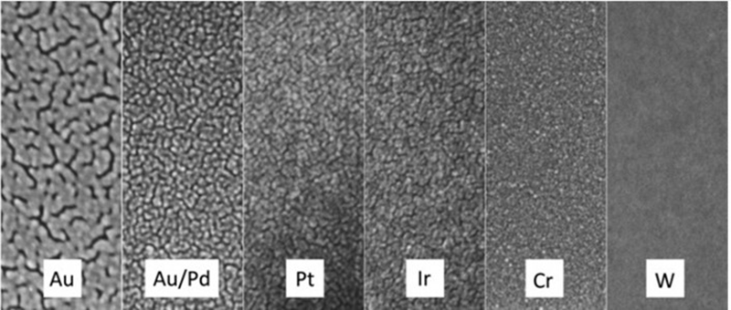
| Target | Grain (nm) | Max Mag | Sputter Rate | Pros | Cons |
|---|---|---|---|---|---|
| Platinum | 2-3 | 50k | Lower sputtering rate than gold | Can show “stress cracking” in presence of oxygen | Most commonly used Finer grains than Au or Au/Pd |
| Gold | 10-12 | 10 k | Fast sputtering | Typically has large islands / grains | Fast Sputter Does not oxidize under air exposure |
| Gold / Palladium alloy (60/40 and 80/20) | 4-8 | 25k | Slightly slower sputter rate than pure Au | Smaller grain size than gold | |
| Amorphous Carbon | No crystalline structure | Appropriate for mag down to TEM | Lower conductivity than the metal options | Best for EDX analysis. C X-ray peak does not overlap other elemental peaks |
Heu, R., Shahbazmohamadi, S., Yorston, J., & Capeder, P. (2019). Microscopy Today, 27(4), 32-36.
Sample specifics
This is especially useful for biological samples. It can also help with samples like plastics that are sensitive the to the energetic SEM beam.
- Non-conductive samples accumulate electrons due to charging.
- Charging artifacts include sample shifting, white or bright spots, swelling, and raster shifts.
- Samples can also be sensitive to the heat imparted by the SEM beam.
Challenges
Once the sample is coated the atomic number contrast visualized on SEM is lost.
Users must test coating parameters to identify optimal conditions for each sample type. We have a standard procedure that is useful for a wide variety of material and can be used as a starting point.
Non-ideal coatings can add false topography, grain structures, or islands.
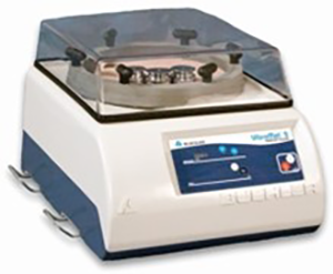
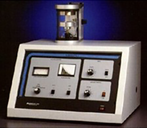
Anatech Hummer 6.2 Sputter Coater
This uses cold temperature deposition where ions dislodge metal atoms from the target. These atoms uniformly coat specimens even with irregular shape or surface variability without causing thermal damage. Coating thickness is controllable, repeatable, and easily controlled.
- Plasma mode : Outgas and clean sample before applying coating
- Etching mode : Removes non-bonded surface material to provide better adhesion
- Plating mode : Coats a specimen with chosen metal
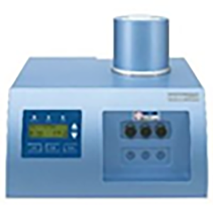
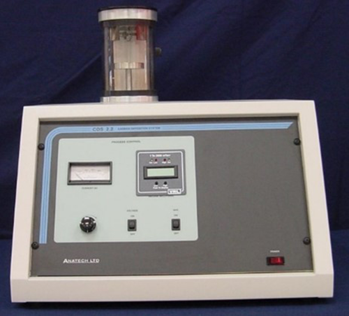
Anatech CDS 2.2 Carbon Sputter Coater
Thermal evaporation of carbon under vacuum using a carbon rod. 100 amps of electrical current is passed between the rod producing resistive heating. Carbon is evaporated from the point and deposited on the sample surface. The vacuum removes oxygen, nitrogen, and water vapor from the coating chamber providing two key features
- Reduced impurities and defects in the film
- Reduced scattering creates an amorphous film of higher purity and density
Chamber can hold samples up to 3.25" diameter or 12 stubs
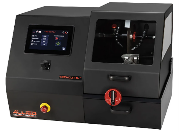
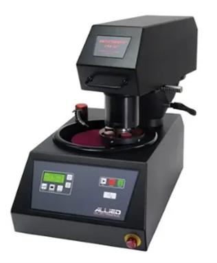
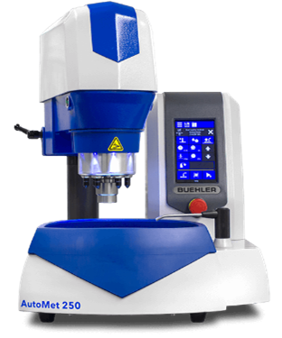
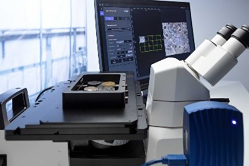
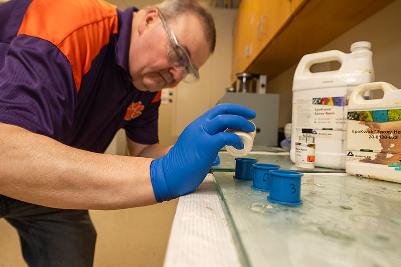
Resin Embedding for Sample Cross-Sections
A variety of resins and mold are provided for sample embedding of different shapes, sizes, and types of samples. Members with experience in these techniques can provide guidance for the best approaches for new samples. Listed is the typical process
- Embed samples in resin mold
- Section the resin to expose desired surface or cross-section with one of the techniques
- Fracture / Freeze fracture
- Microtome Sectioning
- Cutting with abrasive saw
- Cutting / Milling / Polishing with CleanMill Broad Ion Beam System
- Polishing with Grinder/Polisher
- Overnight ultra-fine polishing with Vibromet
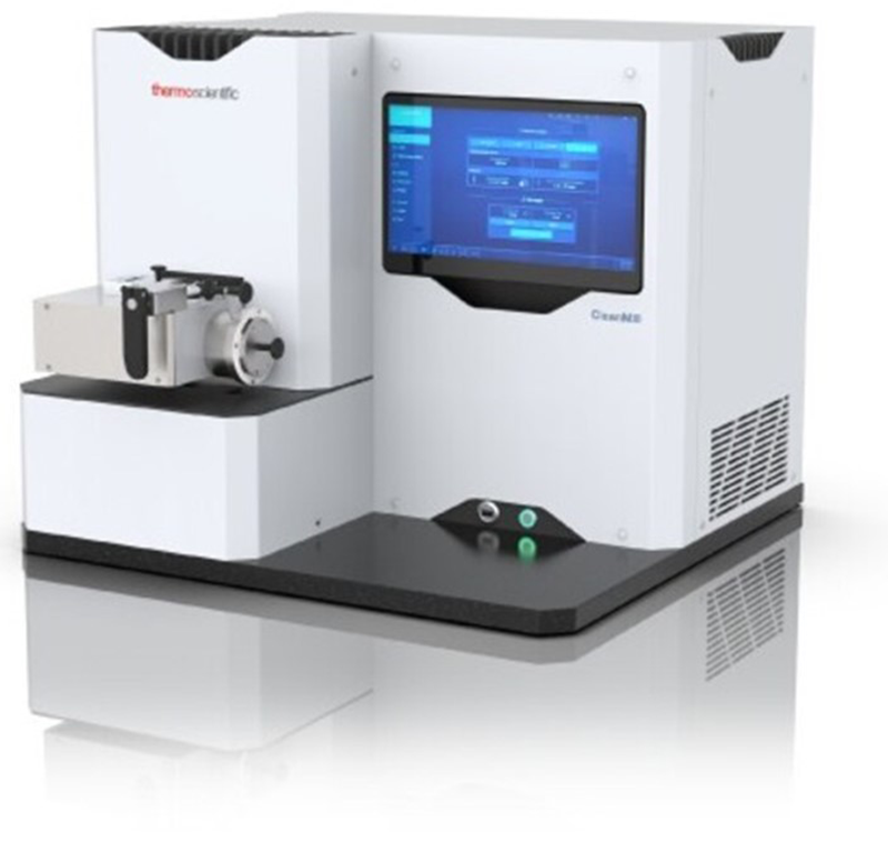
ThermoFisher CleanMill Broad Ion Beam System
Argon Ion beam polishing for a pristine and artifact-free surface preparation for SEM. High throughput and automated for quick and easy sample preparation.
- Rapid cutting / milling / polishing with the 16 kV Ar ion gun.
- Ultra fine surface polishing from 100 V to 2 kV.
- Cryogenic milling with LN2 cooling for beam sensitive materials.
System Parameters
Standard sample preparation : 30 mm (diameter) x 15 mm (height)
Cross section preparation : 90° slope: 10 mm x 10 mm x 3 mm
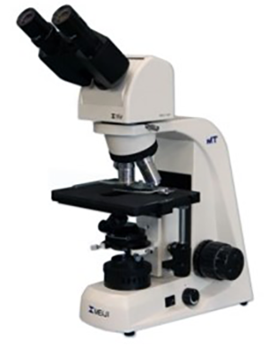
Dedicated optical microscope with CMOS camera 10x optical zoom and 120 x digital zoom
RMC Boeckeler PowerTome X
Ultramicrotome for producing semi and ultra thin sections for TEM, SEM, and TOF SIMS.
- Sections cut to thicknesses of 5 nm – 10 μm
- Cryo- sample preparation is available with this system