General Information
Please refer to the Scanning Electron Microscope Instrument Specifications table (bottom of the page) to find out which microscope is most suited for your requirement by comparing the different features.
Please refer to the Scanning Electron Microscope Instrument Specifications table (bottom of the page) to find out which microscope is most suited for your requirement by comparing the different features.
Fastest and easiest microscope ideal for biological samples or new users
Imaging : SEM
Secondary Electron
Analytical : EDS
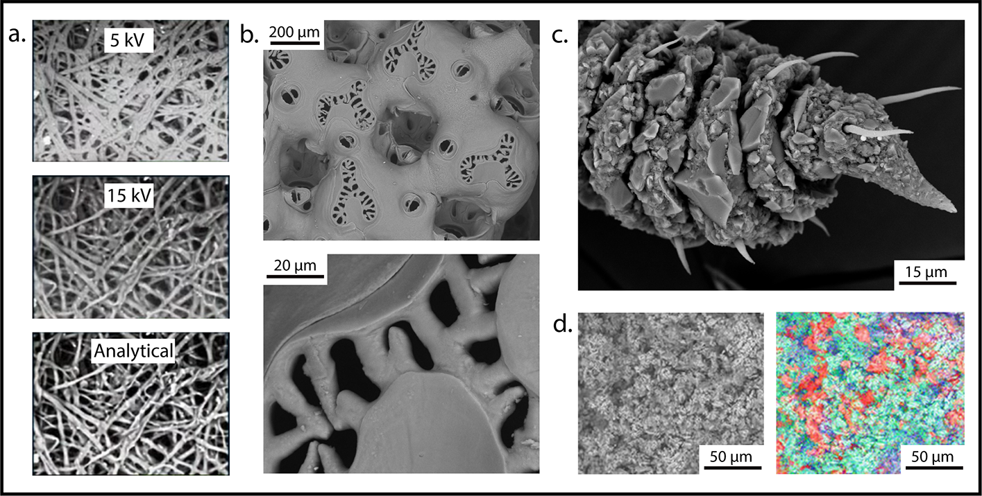
a. Non conductive fibers can be visualized in variable pressure (VP) mode. Imaging is demonstrated at 5kV, 15 kV, and analytical conditions (required for EDX) b. Uncoated bryozoan imaged at 250x in VP mode. The image below shows zoomed in photo of the pores.* c. Nemotode head found in the deep-sea. Nematodes stick fine sediments around them in rings for protection and these structures are clearly identified.* d. EDX mapping of phosphate-calcium cement containing a whisker structure. Green : Ca, Red : Si, Blue : P** e. SE f. BF. ***
*Bryozoan images shared by NIWA.
**Hideaki Narusawa et al. Materials Sciences and Applications Vol.3 No.11(2012), Article ID:24725,5
***All other images reproduced from Hitachi product material.
High resolution variable pressure microscope
Imaging : SEM
Secondary Electron
Five segment BSE detector
Analytical : EDS
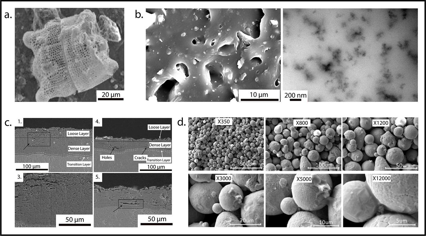
a. SEM of Epiphytic Diatom of Biddulphia pulchella. SEM of this species provides information about morphology and biology of this species found on Seagrass in Palk Strait.* b. Micro SiO2 Silicon Rubber composite (left) is compared to nano SiO2 Silicon Rubber composite. Samples are characterized by SEM cross-section identifying good distribution of the micro and nano particles. Insulating samples were sputter coated with gold.** c. Surface structural features of porous films are identified by SEM images of ZrO2 films formed in (1) silicate electrolyte and (2) phosphate electrolyte. (3&4) Are magnified images respectively.*** d. Stainless steel particles crosslinked by TEG-DMA binder is visualized at multiple magnification levels from 350-1200. Images demonstrate particle packing as well as the crosslinking features of binder necks between particles, excess binder globules, and particles not bound to the matrix.****
*C. Govindasamy, K. Anantharaj, 2012 Environ Sci.
**Muhammad Tariq Nazir, Bao Toan Phung, High Voltage, Vol 3, Issue 4 p. 295-302
***Wang, ZG., Chen, WD., Yan, SF. et al. Rare Met. 41, 1043–1050 (2022).
****Dustin Gilmer et al. Additive Manufacturing, Vol 35, 2020, 101341, ISSN 2214-8604
Large chamber microscope that can operate in a variable pressure and high vacuum modes.
Handles all types of specimens
Imaging : SEM
Secondary Electron
Five segment BSE detector
UV Detector
Analytical : EDS / EBSD / WDX
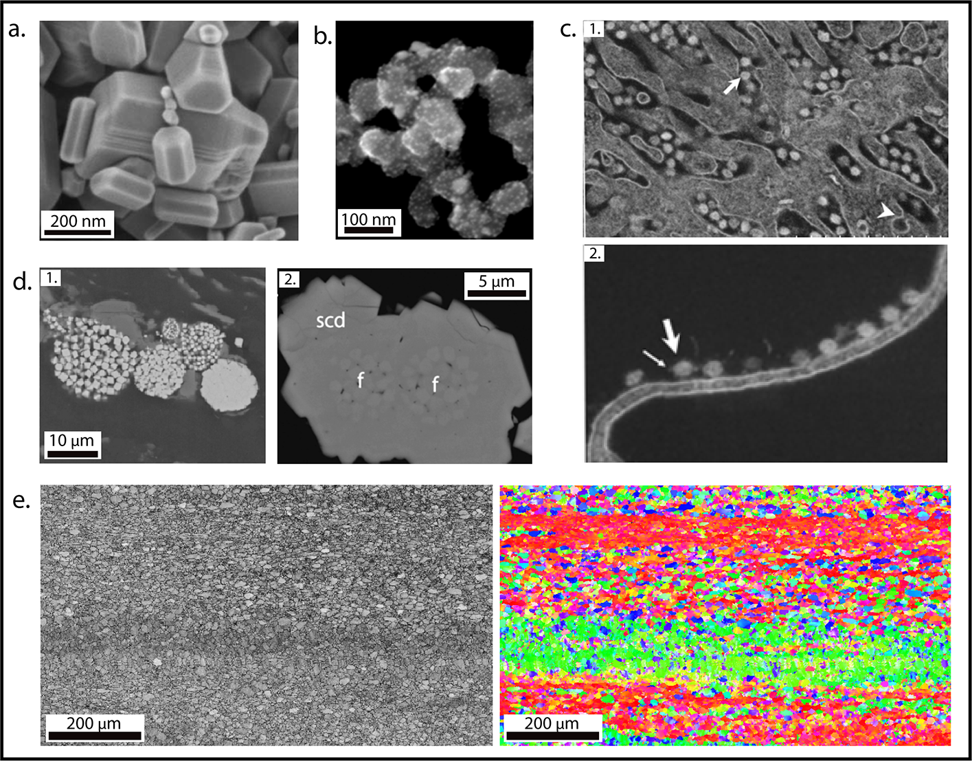
a. High resolution image of Zinc Oxide powder obtained at low kV (1kV). b. Catalyst with metal NPs ~ 2nms are easily distinguished. c. SEM of SARS-CoV-2 particles can be seen (arrows demonstrate example) between microvilli. (1) In the bottom image (2) higher magnification shows the viral particles in vacuoles attached to a plasma membrane. The small arrow indicates corona spike. Cells were fixed and sectioned via ultramicrotome and then sputter coated with platinum. SU5000 was operated in high-vacuum mode at 10 kV. Samples were compared on SEM and TEM demonstrating the ease and speed of data collection on SU5000 compared to a typical TEM viral analysis.* d. BSE image of pyrite (1) collected from Illinois Basin Herrin Coal. (2) Two clusters of pyrite framboids (marked by f) overgrown by secondary pyrite (scd).** e. Grain boundary, size, and shape are identified by Band Contrast EBSD map and inverse figure pole (IPF) – Z. Images are quickly stitched over large areas in several hours.****
*Djamal Brahim Belhaouari et al. Front. Microbiol., 19 August 2020 Virology (11 – 2020)
**Allan Kolker et al. International Journal of Coal Geology, Vol 243, 2021, 103781
***Images collected on SU5000 by Emily Steele, Clemson Electron Microscopy Core
****All other images reproduced from Hitachi product material.
High resolution and variable pressure FE SEM imaging
Imaging : SEM
Secondary Electron
Five segment BSE detector
Analytical : EDS / EBSD
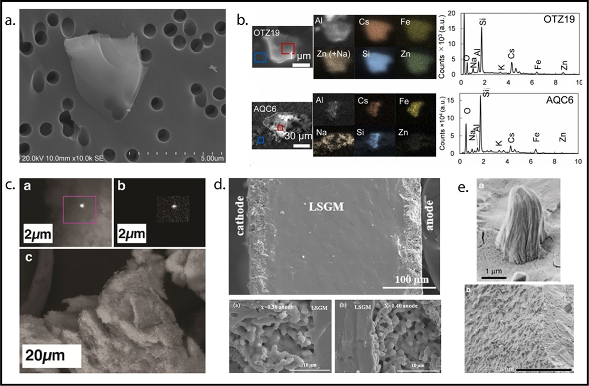
a. SE image of an α-SiC particle. * b. SEM analysis of two Cs micro-particles from Fukushima nuclear reactor control rods. Analysis includes SE image, EDX maps, and EDX spectra.** c. SEM imaging of NP aggregates of silver citrate. (a) Focused image of silver nanoparticles within the aggregate are identified as bright spots (a) and confirmed by EDX mapping (b). In a larger image of the whole aggregate NP are seen distributed throughout the whole aggregate.*** d. Cross-section of single solid oxide fuel cell is analyzed before and after performance test. Changes in microstructure between the cathode and the anode are imaged in (a) and (b) below.**** e. SE of iron whiskers on iron sulfide asteroid surface imaged to track space weathering. (a) Image focused on one whisker compared to (b) wider field view of many iron whiskers. Darker dots on the iron sulfide are open vesicles.*****
*Ervik, T.K., Benker, N., Weinbruch, S. et al.. Anal Bioanal Chem 410, 2711–2721 (2018)
**Kazuki Fueda et al. Journal of Hazardous Materials, Vol 428, 2022, 128214, ISSN 0304-3894
***Hilary P. Emerson et al. J Nanopart Res (2014) 16:2258
****Peng Zhang et al.Journal of Power Sources, Vol 266,2014 (241-249) ISSN 0378-7753
*****Matsumoto, T., Harries, D., Langenhorst, F. et al. Nat Commun 11, 1117 (2020)
High resolution large sample chamber microscope
Bi Cluster Liquid Metal Ion Gun
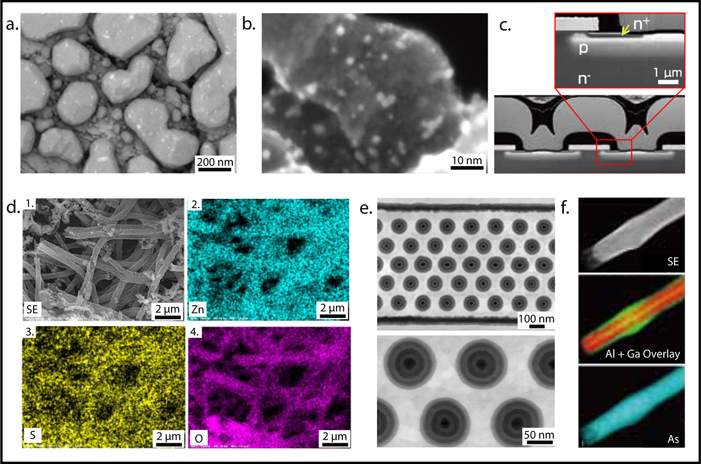
a. Gold nanoparticles on Carbon collected with a landing voltage of 10 V. b. SE image of catalysts with clearly distinguished metal NPs. Demonstrates extended maximum magnification 1,500,000x. c. SiC device demonstrating dopant contrast for imaging p-n function. Inset shows zoom of device structure. d. SE image and EDX chemical map ZnO/ZnS nanofibers prepared by electrospinning and vulcanization. e. SEM of surface of SiN, Poly-Si, and SiO layers concentrically arranged for a memory device.** f. III-V semiconductor nanowire device composed of GaAs-AlAs-AlGaAs. This complex structure is revealed through EDX elemental mapping.***
*Fen Qiao et al. International Journal of Hydrogen Energy, Vol 48, 32023 (953-963) ISSN 0360-3199
**Data collected on SU9000 by STInstruments.
***All other images reproduced from Hitachi product material.
Highest resolution STEM
Bi Cluster Liquid Metal Ion Gun
Imaging : SEM / STEM
Secondary Electron
Low angle BSE
High angle BSE
Dark field / Bright field STEM
Analytical : EDS / EELS
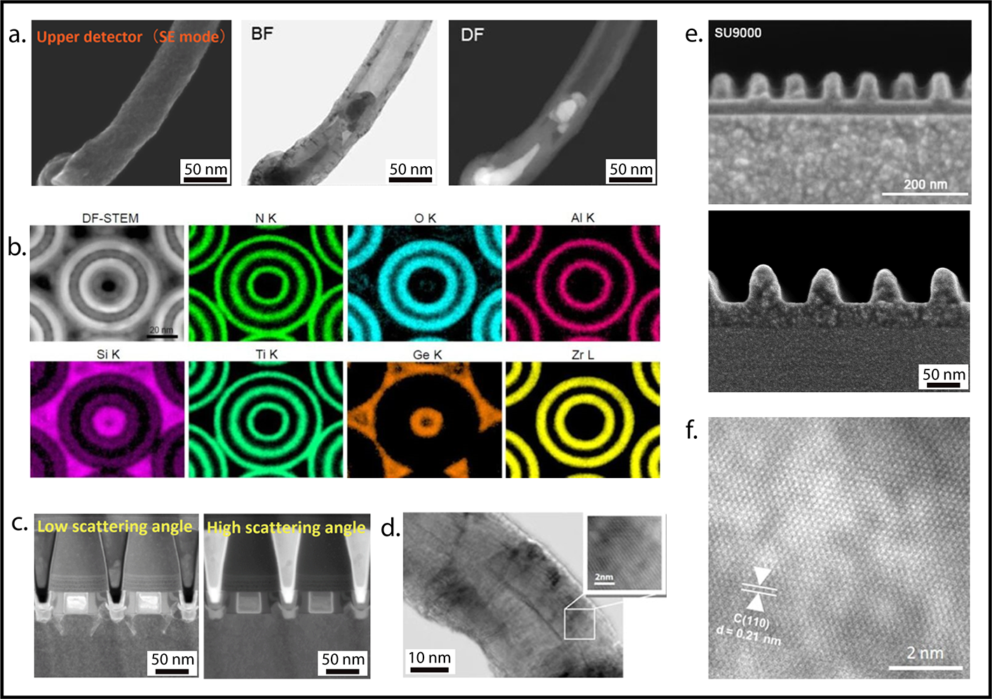
a. The excellent stability of the SU9000 system provides STEM resolution required for nanomaterials. Collection of multiple signals; SE, BF, & DF here are used for elucidating different properties of multiwalled carbon nanotubes (MW CNTs). Secondary electron (SE) signal provides surface based microstructure visualization. Bright Field (BF) detects transmission and provides internal microstructure. Dark Field (DF) detects high angle scattered transmission and visualizes the metal catalyst NPs present inside the CNT. b. Dynamic random-access memory (DRAM) cells composed of capacitors and transistors are packed into dense arrays. High resolution imaging and chemical mapping are rapidly (7 min) collected with a windowless EDX detector. Mapping confirms multilayered packed structures of SiGe, TiN, and ZrO2.* c. n-MOS transistor (n-type Metal Oxide Semiconductor) visualized with low/high angle scattering. The low scattering angle provides surface and topographical information. The high scattering angle image provides chemical information for very small details and crystallinity. The W metal, silicide structures, and nMOS transistors are clearly visualized beneath the surface. d. BF STEM image of multiwalled carbon nanotube with an inset showing the lattice fringes. e. SE image of ArF photoresist nanostructures are visualized with NO beam deceleration (TOP) and WITH beam deceleration (BOTTOM) f. BF STEM image of graphene showing lattice fringe with spacing of 0.21 nm as is expected for crystalline planes of graphene.**
*DRAM cell data collected on SU9000 by STInstruments.
**All other images reproduced from Hitachi product material.
Ga ion beam milling paired with high resolution FE SEM imaging for sample prep and nano fabrication
Imaging : SEM / STEM
Secondary Electron
Back Scatter Electron
Ion imaging secondary ion
Ion-induced SE Imaging
Analytical : EDS / EBSD
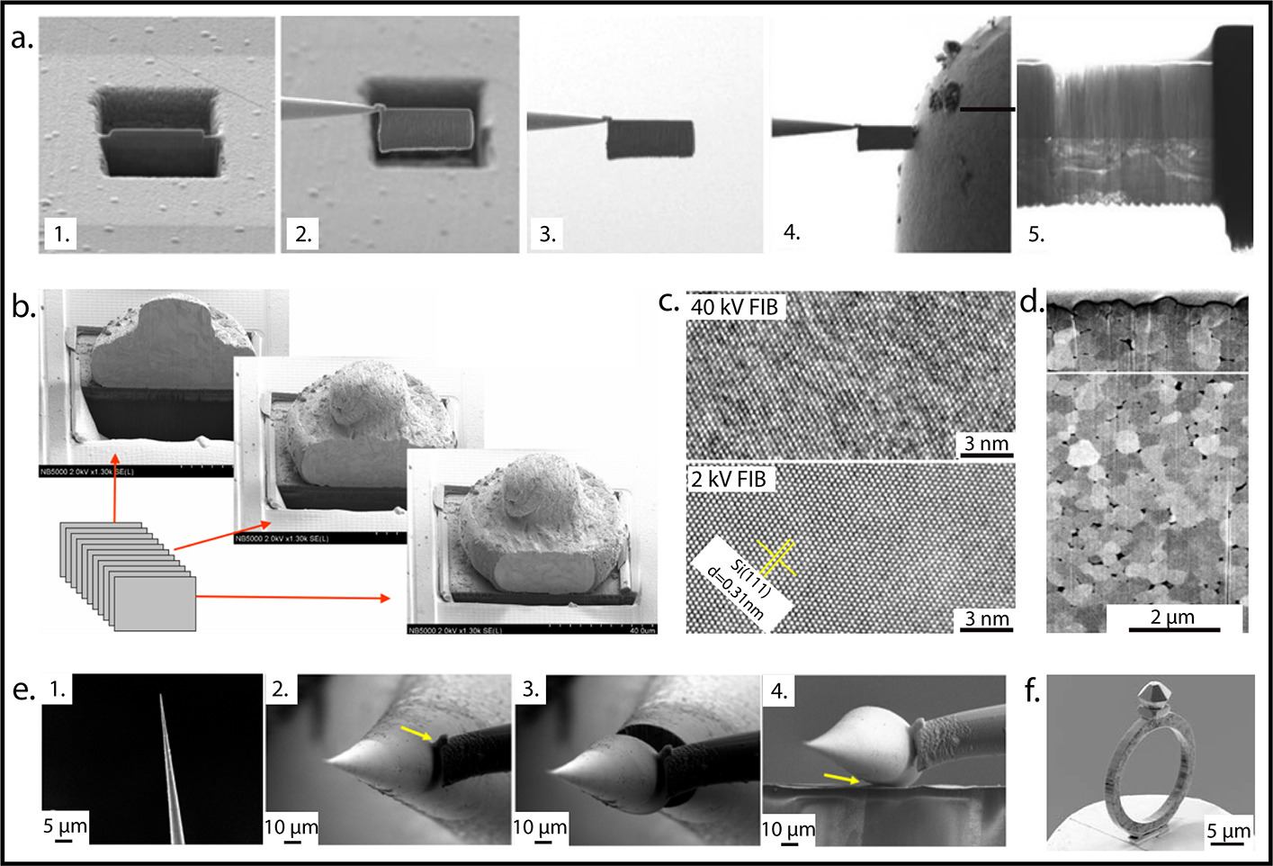
a. FIB Lift Out is the most common use for the NB500. Samples for TEM are prepped by (1) creating a thin section digging two trenches on either side. (2) A micromanipulator probe is attached to the section via a weld. (3) The section is lifted out of the trench and (4) attached to the TEM grid. (5) The section can be further thinned with precision to achieve the desired thickness.* b. The Mill-and-Monitor approach allows samples like this gold ball bond and pad to be sectioned and visualized via SEM. Here slice steps are 10 μm. This cross-section technique can provide visuals of internal components which can be analyzed by EDX. These cross-sections can also be used to reconstruct into 3D images. c. Silicon lattice images are prepared by FIB polishing at 40 kV and 2 kV. d. FIB cross-sections that are thinned can provide grain size and structure information using band contrast EBSD map. e. Nanofabrication of an AFM tip. A tungsten microtip (1) is removed for addition to a quartz tuning force to fabricate an AFM tip. (2) the micromanipulator is welded to the desired region of the tungsten tip and (3) FIB cutting removes this from the bulk. The microtip is then (4) transferred and welded to the quartz substrate. (Welds are made at the yellow arrows) *** f. Nanofabrication is used to carve a micro-ring design.****
*Giurlani W et al. Materials Proceedings. 2020; 2(1):1
**Samodurova A et al. Acta Biomater. 2015 Jan;11:477-87.
***Hatem Labidi et al. Ultramicroscopy, 2015; 158 (33-37) ISSN 0304-3991,
****All other images reproduced from Hitachi product material.
|
|
TM 3000 |
SU 3400 |
SU 5000 |
SU 6600 |
Regulus 8230 |
SU 9000 |
NB 5000 |
|
Resolution |
10 nm |
3 nm |
1.2 nm |
1 nm |
0.7 nm |
0.34 nm |
1 nm |
|
Energy |
5, 15 kv |
3-30 kV |
0.5-30 kV |
0.5-30 kV |
0.5-30 kV |
0.5-30 kV |
30 kV |
|
Magnification |
30k |
300k |
600k |
600k |
2000k |
3000k |
600k |
|
Diameter |
70 mm |
200 mm |
200 mm |
150 mm |
200 mm |
5 mm x 10 mm |
25 mm |
|
Height |
50 mm |
85mm |
80 mm |
40 mm |
40 mm |
5 mm |
5 mm |
|
Insulating Samples* |
OK |
OK |
OK |
OK |
Sputter Coating |
Sputter Coating |
Sputter Coating |
|
EDS** |
10 mm |
10 mm |
80 mm |
50 mm |
50 mm |
80 mm |
10 mm |
|
EBSD |
|
. |
. |
. |
|
|
. |
|
WDX |
|
|
. |
|
|
|
|
|
EELS |
|
|
|
|
|
. |
|
|
STEM |
|
|
|
|
|
. |
. |
|
Source*** |
Tungsten Filament |
Tungsten Filament |
Field Emission |
Schottky Field Emission |
Cold Field Emission |
Cold Field Emission |
Field Emission |
|
Best For |
Rapid initial testing |
Biological samples |
Flexible for most materials |
Flexible for most materials |
Large samples |
Best resolution |
TEM lift-out |
* For insulating samples, our variable pressure microscopes don’t require sputter coating with a conductive material. For all other instruments, we are able to sputter coat insulating samples in the facility.
** Detector window size dictates elemental sensitivity. Our detectors range from 10 mm to 80 mm with the latter producing the efficient data for low concentration elements.
*** Cold Field Emission sources provide the best resolution with the lowest stability over very long runs past 3 hrs. Shottky Field Emission provides the second best resolution but is very stable for long overnight runs. The Tungsten filament sources have the third best resolution and are stable for 2-3 hours.