General Information
Please refer to the Transmission Electron Microscope Instrument Specifications table (bottom of the page) to find out which microscope is most suited for your requirement by comparing the different features.
Please refer to the Transmission Electron Microscope Instrument Specifications table (bottom of the page) to find out which microscope is most suited for your requirement by comparing the different features.
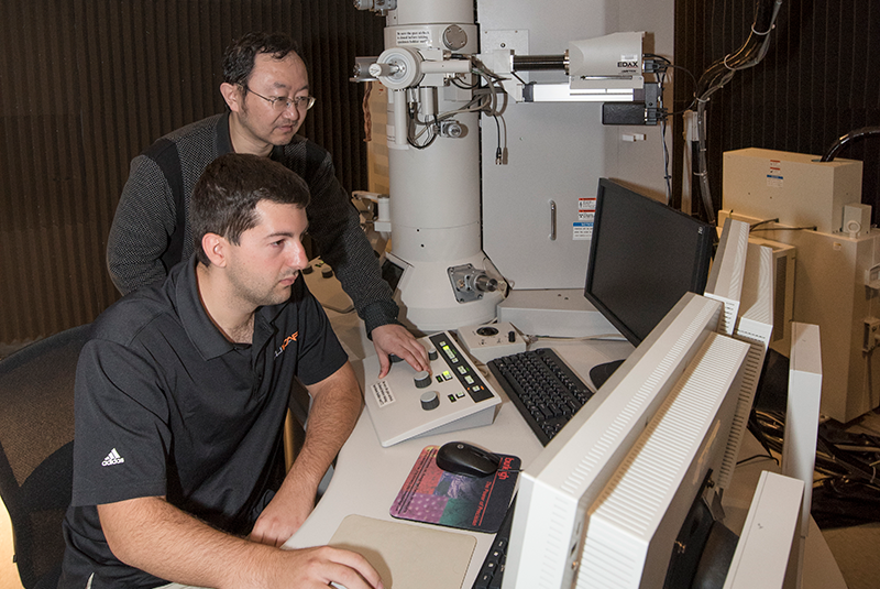
The new Hitachi HT7830 UHR 120kV TEM joins the instrumentation fleet at Clemson AMRL. Procuring the very first unit in the US of this innovative technology, the EM Facility at AMRL is at the very cutting edge of modern EM technologies to serve a diverse array of research. This is the latest and Hitachi’s most advanced TEM designed to operate tunable accelerating voltage range of 20 kV-120 kV. This microscope incorporates Hitachi’s Dual-mode objective lens technology that allows users to image their specimens in a variety of conditions such as low magnification, wide-field high contrast, high resolution, and more—all in one microscope.
Resolution: 0.14 nm at 120 kV
Magnification: x1,000,000
Analytical : EDS
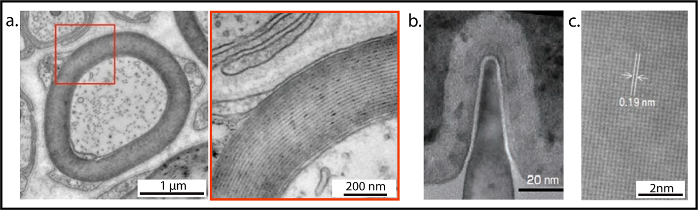
In high contrast mode TEM is ideal for biological specimen visualization. An unstained section of a rat ischial nerve is visualized without applying electron staining. Inset red box shows an enlarged image with a layered myelin structure. b. TEM image of a 22 nm node FinFET device at 300,000x. c. Single crystal silicon with crystal lattice measurement of 0.19 nm.
*Images reproduced from Hitachi product material.
Source: LaB6
Resolution: 0.102 nm lattice; 0.180 point
Magnification:
Zoom1: xx1,000 – xx1,500,000.
Zoom2 (SA): x4,000 – x500,000.
Low Mag: x200 – x500.
Acceleration Voltage: 300keV (standard); 200 keV; 100keV
Analytical: EDS
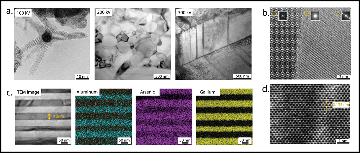
a. Tunable acceleration voltage for different types of materials. Carbon nanotubes at 100 kV. Silicon Nitride at 200 kV. Stainless steel at 300 kV. b. Atomic structural image of silicon lattice resolution of 0.135 nm. c. EDS elemental mapping of TEM region of interest for Gallium Arsenic sample. d. Nano-area diffraction patterns collected from yellow circle areas with a probe diameter of 1 nm. .
|
|
HT7830 |
H9500 |
|
Resolution |
0.14 |
0.102 nm |
|
Acceleration Voltage |
20-120 kV |
300keV, 200 keV, 100 keV |
|
Magnification |
1,000,000x |
1,500,000x |
|
Maximum Stage Tilt |
± 10ᵒ |
± 15ᵒ |
|
Sample Size |
3 mm |
3 mm |
|
EDS* |
80 mm |
. |
|
Heating stage |
|
In situ 900ᵒ |
|
Source |
LaB6 |
LaB6 |
|
Best For |
Biological samples, polymers, and samples sensitive to e- beam damage |
Highest resolution |
* Detector window size dictates elemental sensitivity. Our detectors range from 10 mm to 80 mm with the latter producing the best data for low concentration elements.