Skip to content

Electron Microscopy Facility

Surface Sciences

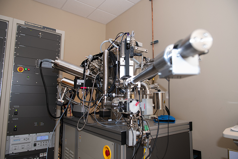
X-Ray Photoelectron Spectroscopy (XPS) – PHI VPIII

Instrument Specifications


Chemical quantification and chemical bonding information from the top ~ 10 nm

  • Angle Resolved analysis between 1nm – 10 nm
  • Ar ion etching (metals / SC)
  • C60+ etching (polymers)
  • In situ heating and cooling
  • Chemical mapping resolution approximately ~ 10 μm

Applications


  • Quantify atomic ratio >0.1%
  • Identify chemical bonding and valence state
  • Depth profile to identify how these factors change through the bulk of the material
  • This can be run in tandem with AES, UPS, LEIPS
  • This can be correlated with TOF-SIMS analysis

XPS Survey and Carbon High Resolution data for PET

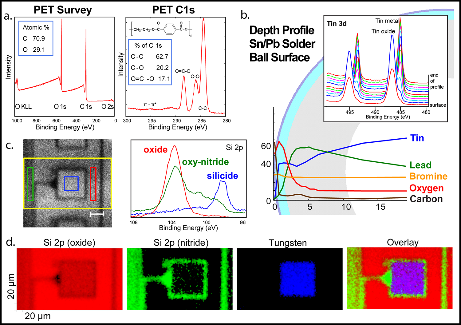
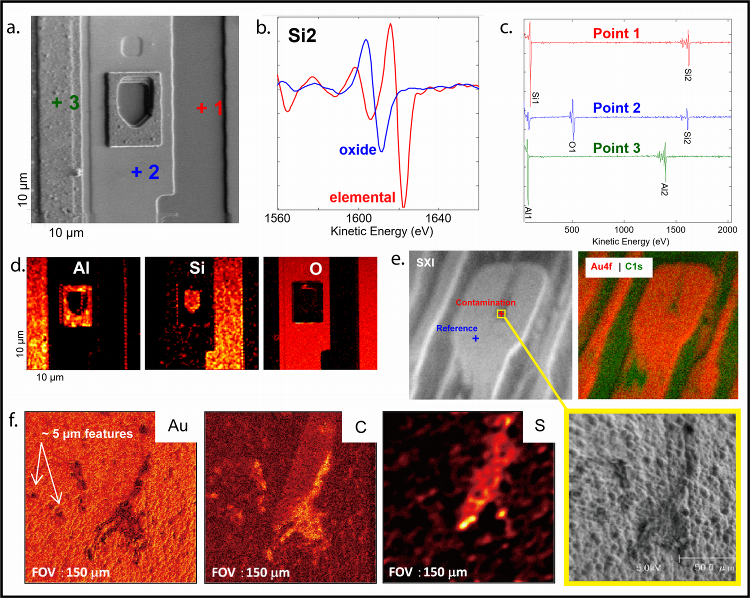
a. XPS Survey and Carbon High Resolution data for PET (Polyethylene Terephthalate). From the survey spectra all elements present at the surface are identified and atomic concentration is calculated. In High Resolution spectra the C-O bonds present can be identified and quantified. b. Ar sputter depth profile of the surface of Sn/Pb solder ball. From atomic concentrations the surface layers can be identified : surface contamination <1nm (dark blue), oxidized layer 2 nm (light blue), lead rich zone >20 nm (grey). The inset shows the Tin high res spectra the oxidized layer can be identified as tin oxide compared to the metallic Tin present in the lead rich zone. c. SXI image of a patterned device marked with three analysis regions. The high resolution Si spectra is color coded for each region oxide (red), oxy-nitride (green), and silicon (blue). d. Chemical mapping of the SXI region from C shows individual elements and species as well as an overlay. Data was mapped with a 10 μm beam.
*All images reproduced from PHI product material.

xps-microscope

researchers with xps-microscope in the lab

Auger Electron Spectroscopy (AES) – PHI VPIII

Instrument Specifications


Chemical mapping from sample surface ~ 2 nm

  • Chemical mapping resolution is ~ 100 nm (compared to ~ 10 μm from XPS)
  • Provides similar data to XPS for analysis requiring smaller spot sizes

Applications


  • Mapping or analyzing small features from nanomaterials, patterns, or contamination
  • Can be paired with depth profiling or sputter cleaning
  • This can be run in tandem with XPS, UPS, LEIPS

Secondary Electron Image (SEI) of a patterned device

a. Secondary Electron Image (SEI) of a patterned device marked with three regions of analysis. b. Auger spectra of Si2 for two regions from A reveals the presence of silicon (1) and silicon oxide (2). c. Auger survey spectra for A indicates the presence of O in 2 corresponding to the oxide. At pt 3 we see the presence of Al. d. Auger elemental mapping images of Al, Si, and O reveals the device structure from the region in A. e. XPS data can be correlated with AES to expand analysis. The SXI image of a region of failure at a bonding pad is marked with two regions for the contamination. The XPS elemental mapping of the pad shows Au (red) at the reference region with high C (green) at the region of contamination. f. AES provides a more focused analysis at the region of contamination (yellow box). Within the C contamination a darker feature is identified and Auger elemental mapping for Au, C, and S shows small S distribution at failure sites.
*All images reproduced from PHI product material.

Ultraviolet Photoelectron Spectroscopy (UPS) – PHI VPIII

Instrument Specifications


Electronic band structure characterization for the valence band

  • Band gap
  • Work /function
  • Structure of the highest occupied molecular orbital

Applications


  • Paired with LEIPS this can provide the full band structure at the sample surface
  • Depth profiling can track the change in electronic properties at different layers
  • This can be run in tandem with XPS, AES, LEIPS

Diagram of UPS and LEIPS

a. Diagram of UPS and LEIPS.* b. UPS of perovskite film (black) and perovskite film with NiOx treated to produce hydrophilic (blue) or hydrophobic surface (red). The secondary electron cutoff (SECO) was used to calculate changes this produced in work function. The valence band edge was used to determine the valence band maximum (VBE) and fermi level.** c. The UPS data for these films (B) were used to create energy level diagrams.** d. Energy level diagram for the interface of PAA and pentacene in pentacene-based MOFETs created from UPS data.*** e. Diagram of the charge transport process for this device (D).*** f. UPS data focused on the SECO and HOMO for the PAA (D) with increasing layer thickness.***
*Reproduced from PHI product material..
**ACS Appl. Energy Mater. 2019, 2, 7, 4890–4899
***Adv Funct Materials, Volume: 30, Issue: 4, First published: 08 November 2019

Low Energy Inverse Photoemission Spectroscopy (LEIPS) – PHI VPIII

Instrument Specifications


Electronic band structure characterization of the conduction band

  • Band gap
  • Ionization Energy
  • Electron Affinity
  • Structure of the Lowest Unoccupied Molecular Orbital

Applications


  • Paired with UPS this can provide the full band structure at the sample surface
  • Depth profiling can be run with LEIPS
  • This can be correlated with XPS and AES data

low energy electron beam

a. Diagram of LEIPS demonstrating low energy electron beam and the emitted near UV photons. This provides information about the energy of unoccupied levels.* b. FIB cros-section of LiCoO2 / LiPON solid state battery.** c. UPS and LEIPS spectra from the LiCoO2 of the battery (B).** d. UPS/LEIPS of the LiPON surface of the battery (B).** e. Diagram of the diffusion and interaction of Ag and bathocuproine (BCP) layer of an organic semiconductor device.*** f. Simulated density of states (Red and Blue lines) with the Kohn-Sham eigenvalues (vertical bars) for BCP-Ag molecular structure shown in (e).*** g. UPS (blue) and LEIPS (red) spectra of BCP-Ag in (e) with arrows marking key spectral features present in both calculated values (f) and the measured spectra*** h. LEIPS spectra for BCP and BCP-Ag complex.*** i. Energy level diagram of the BCP-Ag complex interface with Ag based on the LUMO calculated from LEIPS spectra demonstrating electron transport through the LUMO.***
**Reproduced from PHI product material..
**** S. Iida et al. J. Vac. Sci. Technol. B. 2021;39(4). doi:10.1116/6.0001044
***H. Yoshida, J. Phys. Chem. C 2015, 119, 43, 24459–24464

Time-of-Flight Secondary Ion Mass Spectrometry (TOF-SIMS) – PHI nanoTOF 3

Instrument Specifications


Elemental and molecular imaging from material surfaces ~ 2 nm

Bi Cluster Liquid Metal Ion Gun

  • Spatial resolution 0.07 μm
  • Dual beam charge compensation for insulating sample
  • 5 kV Monatomic Ar source for depth profiling
  • O2 gas source for depth profiling
  • Rapid Imaging 8 kHz
  • High mass accuracy and mass resolution
  • Parallel MS/MS imaging and analysis
  • 3D chemical mapping
  • Inert atmosphere transfer vessel to XPS /UPS

Applications


  • Molecular information of ultra-thin layers, organic materials, tissue sections, and cells
  • 3D reconstruction : Depth profiling paired with chemical mapping
  • Correlate data with XPS, AES, UPS, or LEIPS

TOF SIMS depth profile of Ni-rich layered oxide cathode

a. TOF SIMS depth profile of Ni-rich layered oxide cathode. The species can be divided into the cathode-electrolyte interface and bulk cathode.* b. 3D reconstruction of the NiF3- and 62Ni- depth profile demonstrates the localization of NiF3- at the surface.* c. TOF SIMS mapping before and after sputtering. White arrows mark sputtered region. Mapping indicates F- and C2- are localized at the surface and disappear once the bulk NiO2- signal is exposed. * d. TOF SIMS map of LYZP and LYZP-Li of solid-state batteries. First is an optical image followed by the distribution of P+, PO+, and then the overlay. For the LYZP-Li the map is split into two regions denoted by a dashed blue line marking the LYZP-Li back reaction product and the LYZP pristine surface.** e. Protein loaded PLGA microspheres imaged via TOF SIMS. Anions for PLGA (green), PVA (blue) and lysozyme (red) were mapped to image species distribution at the surface.*** f. TOF SIMS depth profile of key secondary ions in a sulfide rich modified layer on SiO/C anode designed for Li ion batteries. **** g. 3D map of the species distribution demonstrates the different layers present at the interface.**** h. TOF SIMS with amyloid-beta deposits in a hippocampal mouse brain section. The total ion image shows the topography of the surface protrusions. Inset shows measurement of dye p-FTAA (blue) staining the location of the deposits.***** TOF SIMS mapping is correlated with SEM analysis of the surface structure of the identified deposits.****** i. Images of mummy skin cross section collected by TOF SIMS. (1) Map of keratin using ions of leucine, valine, phenylalanine, and tyrosine. (2) Map of collagen using ions of hydroxyproline, proline, glycine, alanine, and glutamic acid. (3) Map of positive calcium ion CaOH+. (4) Overlay of ion images collected from keratin in the epidermis (green), collagen in the dermis (red), and calcium. (blue) j. TOF SIMS imaging of a variety of lipids present at cell membranes prepared for TOF SIMS through different methods; air dried cells (top) and air-plasma treated cells (bottom). *******
* H. Hohyun Sun, Andrei Dolocan, Jason A. Weeks, Adam Heller, and C. Buddie Mullins ACS Nano 2020 14 (12), 17142-17150
** S. Wang, et al. J. Am. Chem. Soc. 2018, 140, 1, 250–257
*** A. Rafati, et al. Journal of Controlled Release, Vol 162, Issue 2, 2012, (321-329) ISSN 0168-3659,
****X. Liu et al. Advanced Science, Volume: 9, Issue: 20, First published: 07 May 2022
***** Solé-Domènech, S., Sjövall, P., Vukojević, V. et al. Acta Neuropathol 125, 145–157 (2013).
******S. Cersoy, et al. J of Mass Spectrometry, Vol 47, Issue 3, 2012 (338-346)
*******H. Lim et al. J. RSC Advances. Issue 49, 2019

scientist with tof-sims microscope

close up of tom-sims-microscope