Micro Fabrication Facility Equipment
Room Detail by Area
The Clemson Micro Fabrication Facility, located within the Advanced Materials Research Laboratory (AMRL) in Anderson, provides a comprehensive suite of state-of-the-art equipment that supports the full spectrum of micro- and nanofabrication processes. From lithography and metal and dielectric deposition to plasma etching, wafer dicing, wet cleaning, and advanced metrology, the facility is equipped to enable precise device fabrication and characterization. These capabilities support a wide range of research and development activities, offering users an integrated environment for designing, fabricating, and analyzing microfabricated structures.
Please log in with your Clemson username and password to make booking requests.
Book Equipment Contact Facility-
Lithography: Resist Coating | UV Exposure
Resist Coater Resist Coating & Developing
Resist Coating Coater
- Semi-automated resist coater with an integrated hot plate
- 100mm tooling
Brewer Sciences Photo Resist Developer Tool
Developer Tool - Semi-automated wafer spin developer with an integrated hot plate
UV Exposure
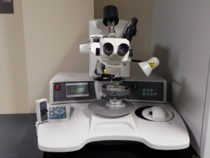
EVG 610 1X Contact/Proximity Printer
EVG 610 1X Model EVG 610 1X aligner
- 3 LED light source, programmable (365, 405, & 436nm exposure wavelengths)
- Currently configured for 100mm wafers
- Mask tooling for 5” masks
- Tooling available for 150mm wafers & 7” masks
- Optical back-to-front alignment capable
- Standard process 1um
- Custom process to 0.40um
GCA 5:1 Reduction i-line optical stepper
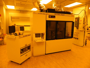
Reduction I-Line Optical Stepper - 0.45na
- 365nm exposure wavelength
- Critical dimension (resolution) 0.5um
- Overlay 150nm XBar + 3 sigma
- Currently configured for 100mm dia. wafers, can expose up to 200mm wafers 0.25mm to 1.0mm thick
- Customized Tooling for exposing 5” X 5” X 0.150” photomasks
- Utilizes 5” X 5” reticles
- Processing of pieces/parts is possible with custom tooling
-
Metal & Dielectric Disposition
Dielectric Deposition
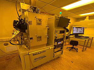
Kurt J Lesker Kurt J Lesker E-Beam Evaporator
Dielectrics:
- Tantalum Pentaoxide
- Silicon Dioxide
- Aluminum Dioxide
- Silicon Monoxide
- Titanium Dioxide
- Hafnium Oxide
Metal Deposition
CCS-CA-40 Evaporator CHA-40 E-Beam evaporator
Metals
- Gold
- Platinum
- Nickel
- Titanium
- Chromium
- Germanium
- Palladium
- Tantalum
- Iron
- Copper
-
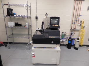
Metrology/Measurement
Metrology
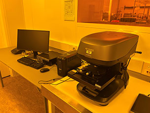
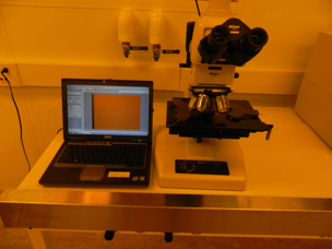
Keyence Microscope - Nikon Optical microscope magnification to 1500X
- Tencor Alpha Step 200 profilometer
- Hitachi S-4800 Scanning electron microscope access on-site at Clemson University's EM facility
- Filmetrics F20 UV Optical thin-film measurement tool
- Keyence VK X3000 Confocal microscope
Nikon Scope 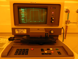
Alpha Step
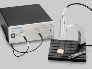
Filmetrics F20 UV Optical Film Thickness Measurement System 
Hitachi SEM -
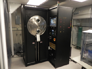
Plasma Etch
Plasma Etch
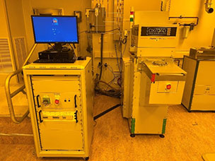
Oxford PlasmaPro ICP Oxford Instruments PlasmaPro 100 Cobra ICP
- Fluorine gases for SiO2, Si, Ge & Ti etching as well as other semiconductor materials
- Configured for 100mm wafers up to 1mm thick
- RIE and or ICP modes
- Primarily used to dry etch SiO2 & Si films and bulk material
Oxford Instruments Plasmalab 100 ICP
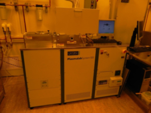
Oxford Plasmalab ICP - Utilizes CL2 & BCL3 etch chemistry for metal or dielectric etching
- Configured for 100mm wafers up to 1mm thick
- Tool can etch up to 10mm thick wafers with optional tooling
- RIE and or ICP modes
- Currently used to dry etch Sapphire & GaAs, As2S3 ,ZnSe, ZnS, Al, & Ni
-
Wafer Dicing: Wafer Dicing | Thermal Evaporation
Wafer Dicing
Wafer Dicing
K&S Dicing Saw K&S Wafer Dicing Saw
- Model 780
- 200mm capable
- Cuts silicon, sapphire & optical glasses
Thermal Evaporation (MBE)
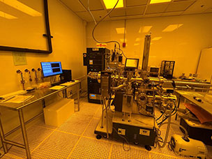
SVTA Cleaving System SVTA Cleaving system w/thermally deposited passivation
The SVTA cleaving system is designed for cleaving wafers into thin strips/bars under ultra-high vacuum (UHV) conditions. The deposition block can then be transferred to a deposition chamber for facet coating of the two cleaved edges or for other deposition processes. This process ensures a mirror edge free from contaminants, a critical requirement in high-performance laser diodes.
-
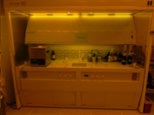
Wet Chemistry/Cleaning
Wafer Cleaning & Wet Etching
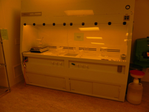
Acid Bench 3 wet hoods from Salare Systems in NC for solvent, acid & base etching and wafer cleaning
Acid Processes
- HCL & H2O2 RCA II cleaning.
- Piranha resist strip (NanoStrip 2X also available)
- SiO2 etch (HF)
- Chrome etch. (CR-7)
- Tungsten etch.
- Gold etch. (GE 8148)
- Platinum etch. (Aqua Regia)
- Nickel etch (HNO3 + Perfluoroalkyl Sulfonate)
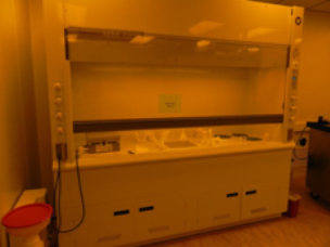
Base Cleaning Bench Base processes:
- Ammonium Hydroxide & Hydrogen Peroxide (RCA I clean)
- Sodium Hydroxide
- TMAH & Na2SiO3 developing
Solvent Hood Processes:
- NMP
- Acetone
- Methanol
- IPA
- PGMEA
Solvent Bench Additional Wet Hoods
- Hydrochloric Acid & Hydrogen Peroxide (RCA II cleaning)
- Sulfuric acid, Hydrogen Peroxide (Piranha Strip)
- NMP, Acetone & Methanol (Solvents)
- Ammonium Hydroxide & Hydrogen Peroxide (RCA I cleaning)
- Additional Services: Wire Bonding | Custom Tooling