CAMMP
Clemson Advanced Manufacturing and Materials Processing
Research themes:  Clemson Advanced Manufacturing and Materials Processing laboratory is expanding the boundaries of knowledge and industrializing novel emerging technologies in manufacturing research. We work on interdisciplinary research, integrating experimental studies and physical modeling of advanced manufacturing and materials processing. My research themes, particularly, are the scalable manufacturing of high-performance, lightweight nanocomposites, smart manufacturing using intelligent devices with self-diagnostic capabilities, and laser material processing for additive manufacturing.
There are three research areas: the design of micro/nano thin film sensors and their integration with manufacturing systems for real-time condition monitoring of processes; fundamental understanding of the behavior of nanomaterial at the interface and the processing-structure-property relationship for liquid-based manufacturing of lightweight nanocomposites; laser-material interaction in deposition and machining processes for direct writing and additive manufacturing. We are also researching the design, multi-physics modeling, and prototype development of scale-up hybrid mixing systems using ultrasonic cavitation and acoustic streaming for metal matrix nanocomposite powders for the powder bed fusion process of heterogeneous meta-material components.
Lab facility/equipment: A partial list of facilities and equipment of Clemson Advanced Manufacturing and Materials Processing laboratory includes:
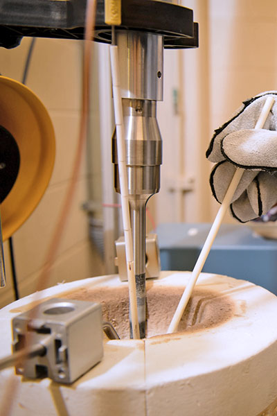
- A 1070 nm fiber laser with a maximum power output of 200 W is implemented to fabricate additive manufacturing (AM) samples via the powder bed fusion process. 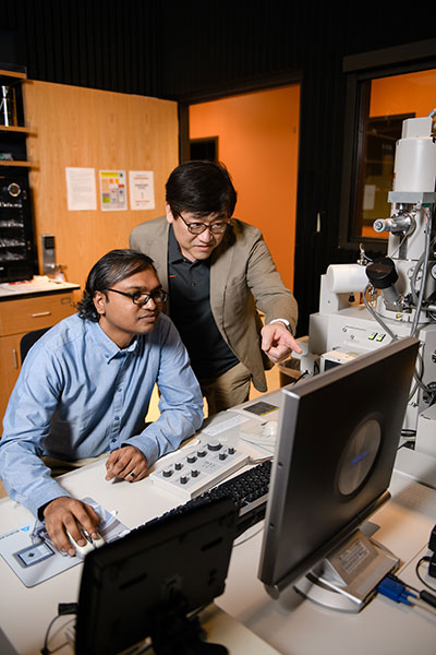 A laser beam is delivered to the surface of a layer of micro powder through a galvanometer-type scan head with a maximum speed of 12 m/s. The microhardness of the fabricated AM samples is measured with an HVD-1000AP microhardness tester. Specimens for micro- and nanostructure analysis will be prepared through sectioning, mounting, grinding, and polishing. An optical microscope and a stereoscope will be used to study the grain structures of AM samples. Inner micro-and nanostructures can be further investigated with high-resolution transmission electron microscopy (TEM, Hitachi H-9500), scanning/transmission electron microscopy (S/TEM, Hitachi HD-2000), and scanning electron microscopy (SEM, Hitachi S-3400) with energy-dispersive X-ray spectroscopy (EDS) and electron backscatter diffraction (EBSD), which can be done in our Advanced Material Research Laboratory (AMRL).
-  500 watts and 1375 watts ultrasonic processing systems are used to mix nanopowders with a large volume of metal melts or polymer solutions to manufacture high-performance, lightweight nanocomposites. A fume hood with carbon and HEPA filters is used to manipulate micro-and nanomaterials. In addition, an electrospinning system is placed inside the fume hood. The inert atmosphere electric melting furnaces are used to prepare a metal melt.
- Thin film microsensors, such as thin film thermocouples (TFTCs), 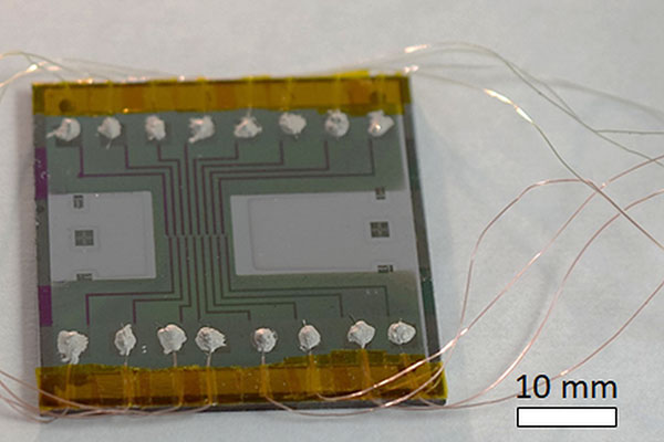 thin film heat flux sensors (TFHFs), and thin film strain gages (TFSGs), fabricated on different types of substrates are calibrated with quartz tube furnace or box furnace with a data acquisition system. The sensors are integrated into a manufacturing system and measure temperature, heat flux, and strain for in-situ process monitoring.
Hongseok Choi
Lab Director
(864) 656-5645
hongc@clemson.edu